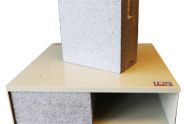
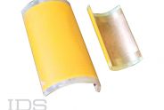
Smart materials can offer many possibilities in the field of electromagnetic engineering. Other than off-the-shelf products, IDS can provide tools and services for analysis and design, up to the complete development of custom products.
The IDS EM modeling and simulation software provides high-fidelity modeling at any working level, from parametric analysis and design/optimization of the smart material to the optimal installation on a platform. A specific smart material design tool based on a periodic Method of Moment solver is available for periodic configurations with both parametric and non-parametric shapes. 2.5D and 3D full-wave solvers, capable of effectively managing tens of millions of degrees of freedom (DoF), are available in an electromagnetic toolkit for non-periodic material configurations and for platform or building installations. Isotropic and anisotropic homogenized equivalent models (HEM) (e.g. reflection/transmission coefficients, penetrable and/or impenetrable surface impedance etc.) can be applied to speed up the computation.
- Assessment of detailed technical specifications from customer requirements
- Concurrent design, to simultaneously manage electrical, mechanical, environmental and thermal requirements
- Design camouflaging
- Prototyping and verification through in-house performance measurements
- Assessment of applicable technological processes (performance vs. cost)
- Cooperation in the definition of “structural smart materials” (i.e. smart components embedded in customers’ composite structures)
- Product qualification vs. standards
- Cooperation in the engineering of industrial processes for large production
- Investigation, training and qualification activities of local manufacturers on-behalf of the customer
- Modeling and engineering support for optimal installation (e.g. to install RAM panels only where really needed to satisfy requirements)
- Installation and on-site verification: product installation can be verified on-site by IDS technical services using portable measurement systems
Main Features
- Comprehensive suite of in-house developed electromagnetic modeling tools
- Smart material analysis and design services covering the full development cycle
- Capability and experience of developing custom smart materials on the basis of customer requirements
- In-house measurement systems and the capability to provide qualification services
Main Benefits
- Availability of theoretical know-how, advanced modeling/design software tools and measurement systems, and well proven experience, all in one place
- Extensive experience in the fields of naval, aeronautical and space platform design as well as air navigation (airport site control)
- Continuous R&D activities to improve our capabilities in the areas of computer aided design and optimization methods, technological solutions, manufacturing processes and diagnostics
- Regular collaborations with research institutions (e.g. European Space Agency and Italian MoD) and universities (e.g. Univ. of Pisa, Univ. of Siena, Polytechnic of Turin, Univ. of Montreal)


